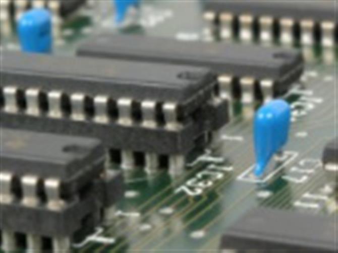
Basic components of SMT processing
The SMT processing flow consists of several key steps: screen printing, placement, soldering, cleaning, testing and maintenance. In the screen printing segment, thesilkscreen machineResponsible for uniformly printing the solder paste or mounting adhesive onto the printed circuit board. Subsequently, themounting machinePlacing the electronic components precisely in the predetermined positions and through thecuring ovenFirm bonding of components to circuit boards is realized in the soldering process. Throughout the process, the setup of repair stations helps to detect and repair defective products in time to ensure product quality.
Product Applications
SMT processing technology is applicable to a wide range of electronic product lines, including but not limited to:
- Wireless communication series: Cordless phone motherboard, wireless public phone motherboard, etc.
- Household electric series: DVD motherboard, CD motherboard, etc.
- Electronic toys series: remote control cars, electronic pets, etc.
- Computer peripheral series: network card, video card, U disk, etc.
Handling Precautions
Standardization of operations and operator safety are critical in SMT processing. Understanding and implementing electrostatic discharge (ESD) protection measures and following the design intent and established standards for SMT processing are key to ensuring product quality. Operators who are unfamiliar with these standards should learn by reviewing the relevant literature.
Welding Assessment Criteria
Soldering is a fundamental part of SMT processing and includes both general and manual soldering. Selection of the appropriate soldering method should be based on evaluation criteria rather than subjective judgment. Highly technical factories may even use 3D build techniques to enhance the appearance and standardization of their products.
Advantages of SMT processing
- High assembly density: Compared with conventional components, SMT technology significantly reduces the area and mass occupied by components, resulting in a reduction in the size of electronic products by 60% and a reduction in mass by 75%. For example, a 64-pin DIP integrated block occupies only 1/12 of the area occupied by conventional technology under SMT technology.
- high reliability: Because the components are small and lightweight, they are highly resistant to vibration, automated production improves placement reliability, the rate of defective solder joints is extremely low, and the Mean Time Between Failure (MTBF) of electronic products is significantly improved.
- Excellent high frequency characteristics: SMT technology reduces the effects of parasitic inductance and parasitic capacitance, improving the high-frequency characteristics of circuits and making them suitable for higher-frequency circuit design.
- cost-effectiveness: The reduction in component size and mass reduces the area used for printed boards and the number of holes drilled, saving material and production costs. With the rapid development of SMC and SMD, its cost is also decreasing rapidly.
- Facilitates automated production: SMT technology is easier to automate than traditional perforated mounting, increasing production efficiency and assembly density.