I. PCB board material
The choice of material for PCB boards has a significant impact on the performance and cost of electronic products:
- tinplate: Known for its low cost and good solderability, but not suitable for lead-free processes due to its lead content.
- tinned board: It is easy to be polluted and scratched, and oxidization and discoloration may occur in the process, which is less used domestically and has a higher cost.
- metalized sheet: There is the problem of "black pads", which are not recommended by some major manufacturers for lead-free processes, although they are still used by some domestic manufacturers.
- silver platingOrganic Silver" technology solves the problem of silver migration and meets the needs of lead-free processes with long solderability life.
- OSP board: Lowest cost, easy to operate, but requires assembly plant to adjust equipment and process, poor reproducibility, protective film may be damaged after high temperature, affecting solderability.
- gold-plated sheet: Highest cost, good stability, suitable for lead-free processes, recommended for high value or high reliability requirements of electronic products.
Second, PCB board composition
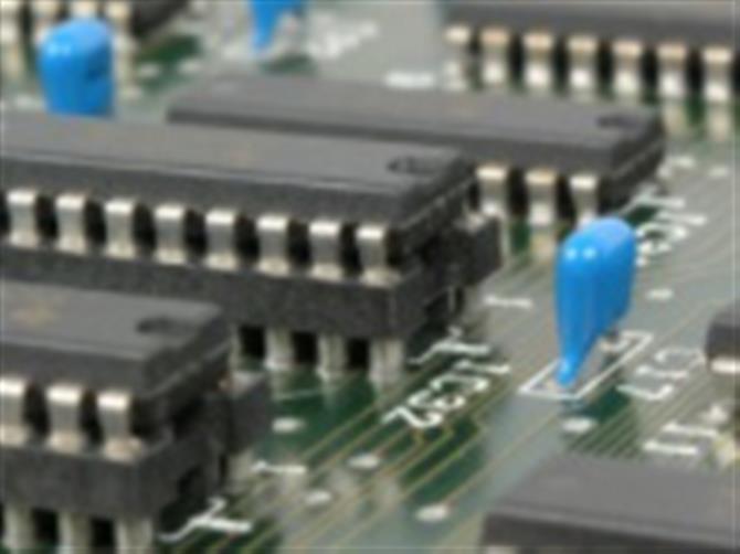
The PCB consists of the following key components:
- Lines and drawings: The wiring serves as a means of conduction between components, and is usually accompanied by a large copper surface that serves as a ground and power layer.
- dielectric layer: Maintaining insulation between lines, commonly known as substrate.
- holes: Conductive holes for multi-layer line connections, large holes for inserts, and non-conductive holes for positioning or fixing.
- Solder Resist Ink: Prevents oxidation of copper surfaces in non-soldered areas and is available in a variety of colors.
- silkscreen: Labeled with part names and locations for ease of maintenance and identification.
- surface treatment: Protects copper surfaces from oxidation and improves solderability, including a variety of treatments.
Third, PCB board production process
PCB board fabrication is a delicate process:
- Printed Circuit Diagrams: Select the best printed circuit diagram for transfer.
- Cutting Copper Clad Laminate: Cut to desired size to save material.
- Pre-treated Copper Clad Laminate: Removes oxidized layers and ensures transfer results.
- Transfer Circuit Diagram: Align and transfer to copper-clad boards, observing safe handling.
- Corrosion of circuit boards: Check the integrity of the transfer and use an etching solution to remove the exposed copper film.
- drilled hole: Select the appropriate drilling needles according to the thickness of the component pins and pay attention to the stability of the operation.
- preprocessing: Remove toner, wash and dry, apply rosin.
- Soldering of electronic components: Component soldering is completed and power-on testing is performed.