The Importance of PCBA Design for Manufacturability
The design of PCBAs for manufacturability is not only about the manufacturing feasibility of the product, it is also the key to realizing the goal of low-cost, high-quality production. The realization of such a design depends on careful consideration during the design phase and close coordination with the manufacturing process. Recognizing the "integration" of design and manufacturing is critical to good PCBA design for manufacturability.
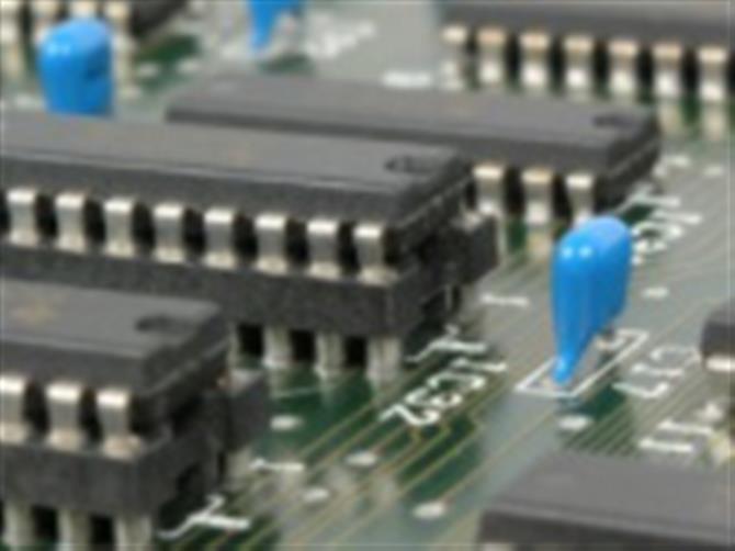
Core Elements of Design for Manufacturability
In SMT, design for manufacturability typically involves design elements such as optically positioned symbols, transfer edges, assembly methods, spacing and pads. The real challenge, however, is how to effectively "harmonize and unify" these elements. Without this understanding, even if a single design element meets the criteria, it may not achieve the desired manufacturing results.
Steps in PCBA Design for Manufacturability
- Determine assembly method based on BOM: First, according to the number of components and package types in the Bill of Materials (BOM) of the hardware design, determine the assembly method of the PCBA, which includes the layout of components on the front and back sides of the PCBA, which directly affects the process path design.
- Soldering Process Methods Guide Component Layout: Different soldering processes have specific requirements for component layout. For example, wave soldering requires that the long edges of the chip components be perpendicular to the direction of transfer and that the component spacing be greater than the height of neighboring components.
- Encapsulation matching to pads, stencil openings: The process characteristics of the package determine the amount of solder paste required and its distribution. The package, the pads and the stencil window are interconnected, the pad and pin structure influences the shape of the solder joint and the absorption capacity of the molten solder, while the stencil window and thickness design determines the amount of solder paste to be printed.
Design for Manufacturability and Manufacturing Yield
Design for manufacturability provides the basis and inherent process capability (Cpk) for high quality production, echoing the quality management concept of "design determines quality".
Integrated design concept
When designing for manufacturability, it is important to keep these intrinsically linked perspectives in mind and to consider the design elements in an "integrated" way to ensure that the design not only meets the manufacturing requirements, but also achieves the goals of low-cost and high-quality production.